Publications 2011 - 2014
2014
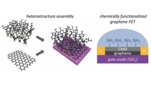
Scheme of the heterostructure assembly (left) and the chemically functionalized graphene FET (right).
Image: Wiley-VCH: Advanced MaterialsM. Woszczyna, A. Winter, M. Grothe, S. Wundrack, R. Stosch, T. Weimann, F. Ahlers, A. Turchanin
All-carbon vertical van der Waals heterostructures: Non-destructive functionalization of graphene for electronic applications
ADVANCED MATERIALS 2014, 26, 4831-4837
DOI: 10.1002/adma.201400948External link
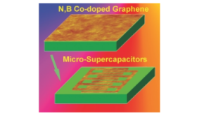
Schematic representation of the doped Graphene before and after structuring
Image: Wiley-VCH: Advanced MaterialsZh.-Sh. Wu, K. Parvez, A. Winter, H. Vieker, S. Han, A. Turchanin, X. Feng, K. Müllen
Layer-by-layer Assembled Heteroatom-Doped Graphene Films with Ultrahigh Volumetric Capacitance and Rate Capability for Micro-Supercapacitors
ADVANCED MATERIALS 2014, 26, 4552-4558
DOI: 10.1002/adma.201401228External link
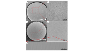
HRTEM images showing the effect of dry-cleaning of graphene with activated carbon.
Image: AIP Publishing: Applied Physics LettersG. Algara-Siller, O. Lehtinen, A. Turchanin, U. Kaiser
Dry-cleaning of graphene
APPLIED PHYSICS LETTERS 2014, 104, 153115
DOI: 10.1063/1.4871997External link
2013
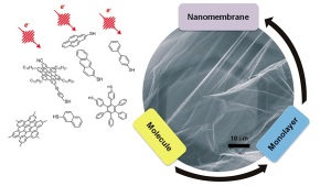
Schematic representation of different precursor molecules used for CNM synthesis and the procedure from single molecules to a Nanomembrane
Image: ACS Publications: ACS NanoP. Angelova, H. Vieker, N.-E. Weber, D. Matei, O. Reimer, I. Meier, S. Kurasch, J. Biskupek, D. Lorbach, K. Wunderlich, L. Chen, A. Terfort, M. Klapper, K. Mullen, U. Kaiser, A. Gölzhäuser, and A. Turchanin
A Universal Scheme to Convert Aromatic Molecular Monolayers into Functional Carbon Nanomembranes
ACS NANO 2013, 7 6489-6497
DOI: 10.1021/nn402652fExternal link
There is a "Perspective" in ACS Nano about our article written by R.E. Palmer, A.P.G. Robinson, and Q. Guo:
How Nanoscience Translates into Technology: The Case of Self-Assembled Monolayers, Electron-Beam Writing, and Carbon NanomembranesExternal link
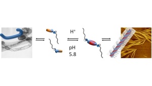
Zwitterions forming Dimers and Nanostructures as a consequence of pH-changes
Image: ACS Publications: Journal of the American Chemical SocietyM.T. Fenske, W. Meyer-Zaika, H.-G. Korth, H. Vieker, A. Turchanin, C Schmuck
Cooperative Self-Assembly of Discoid Dimers: Hierarchical Formation of Nanostructures with a pH Switch
JOURNAL OF THE AMERICAN CHEMICAL SOCIETY 2013, 135, 8342-8349
DOI: 10.1021/ja4025148External link
Frontispiece of Advanced Materials Volume 25, Issue 30
Picture: Wiley-VCH: Advanced Materials
D. G. Matei, N.-E. Weber, S. Kurasch, S. Wundrack, M. Woszczyna, M. Grothe, T. Weimann, F. Ahlers, R. Stosch, U. Kaiser, A. Turchanin
Functional single-layer graphene sheets from aromatic monolayers
ADVANCED MATERIALS 2013, 25 4146-4151
DOI: 10.1002/adma.201300651External link
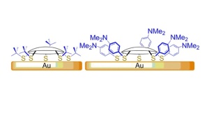
Schematic representation of two corannulene derivatives synthesised.
Image: ACS Publications: LangmuirPolina Angelova, Ephrath Solel, Galit Parvari, Andrey Turchanin, Mark Botoshansky, Armin Gölzhäuser, and Ehud Kienan
Chemisorbed Monolayers of Corannulene Penta-Thioethers on Gold
LANGMUIR 2013, 29, 2217-2223
DOI: 10.1021/la304600sExternal link
2012
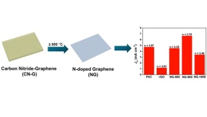
Thermal conversion of Carbon Nitride-Graphene to n-doped Graphene,as well as the electrochemicalactivity given as the kinetic-limiting current density for different nanocrystaline graphene electrodes
Image: ACS Publications: ACS NanoK. Parvez, S. Yang, Y. Hernandez, A. Winter, A. Turchanin, X. Feng, K. Mllen
Nitrogen-Doped Graphene and Its Iron-Based Composite As Efficient Electrocatalysts for Oxygen Reduction Reaction
ACS NANO 2012, 6, 9541-9550
DOI: 10.1021/nn302674kExternal link
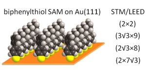
Spherical Model of biphenylthiol SAM on Au(111)
Image: ACS Publications: LangmuirD. G. Matei, H. Muzik, A. Gölzhäuser, and A. Turchanin
Structural Investigation of 1,1'-Biphenyl-4-thiol Self-Assembled Monolayers on Au(111) by Scanning Tunneling Microscopy and Low-Energy Electron Diffraction
LANGMUIR 2012, 28, 13905-13911
DOI: 10.1021/la302821wExternal link
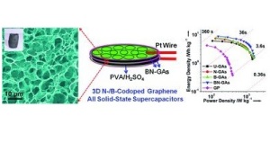
A simplified prototype device of high‐performance all‐solid‐state supercapacitors (ASSSs) based on 3D nitrogen and boron co‐doped monolithic graphene aerogels.
Image: Wiley-VCH: Advanced MaterialsZh.-Sh. Wu, A. Winter, L. Chen, Y. Sun, A. Turchanin, X. Feng, K. Mllen
Three-dimensional nitrogen and boron co-doped graphenes for high-performance all solid-state supercapacitors
ADVANCED MATERIALS 2012, 24, 5130-5135
DOI: 10.1002/adma.201201948External link
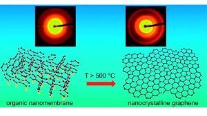
structure of organic nanomembranes (left) and, after thermal conversion, nanocrystaline graphene, including their respective diffraction patterns
Image: ACS Publications: The Journal of Physical Chemistry CD.C. Rhinow, N.-E. Weber, A. Turchanin
Atmospheric Pressure, Temperature-Induced Conversion of Organic Monolayers into Nanocrystalline Graphene
THE JOURNAL OF PHYSICAL CHEMISTRY C, 2012, 116, 12295-12303
DOI: 10.1021/jp301877pExternal link
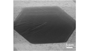
Helium Ion Microscopy (HIM) image of a 1 nm thick CNM covering a hexagonal pore (∼40 μm in diameter).
Image: Elsevier: Progress in Surface ScienceA. Turchanin, A. Gölzhäuser
Carbon nanomembranes from self-assembled monolayers: Functional surfaces without bulk
PROGRESS IN SURFACE SCIENCE, 2012, 87, 108-162
DOI: 10.1016/j.progsurf.2012.05.001External link
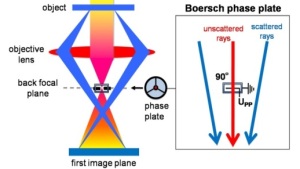
Phase contrast TEM with a BPP. The BPP is an electrostatic einzel lens that shifts the phase of the unscattered beam by 90° to maximise in-focus phase contrast of weak-phase objects.
Image: Elsevier: UltramicroscopyA. Walter, H. Muzik, H. Vieker, A. Turchanin, A. Beyer, A. Gölzhäuser, M. Lacher, S. Steltenkamp, S. Schmitz, P. Holik, W. Kühlbrandt, D. Rhinow
Practical aspects of Boersch phase contrast electron microscopy of biological specimens
ULTRAMICROSCOPY, 2012, 116, 62-72
DOI: 10.1016/j.ultramic.2012.03.009External link
2011
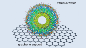
Ice-embedded TMV on nanocrystalline graphene.
Image: American Institute of Physics: Applied Physics LettersD. Rhinow, N.-E. Weber, A. Turchanin, A. Gölzhäuser, W. Kühlbrandt
Single-walled carbon nanotubes and nanocrystalline graphene reduce beam-induced movements in high-resolution electron cryo-microscopy of ice-embedded biological samples
APPLIED PHYSICS LETTERS , 2011, 99, 133701
DOI: 10.1063/1.3645010External link
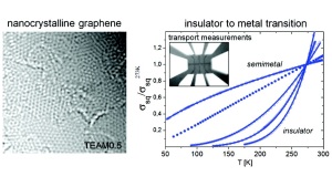
left: high-resolution transmission electron image of nanocrystaline graphene, right: Experimental σ(T) data for the experimental samples annealed at different temperatures after normalization to σ(273K)
Image: ACS Publications: ACS NanoA.Turchanin, D. Weber, M. Benfeld, C. Kisielowski, M. V. Fistul, K. B. Efetov, T. Weimann, R. Stosch, J. Mayer, A. Gölzhäuser
Conversion of Self-Assembled Monolayers into Nanocrystalline Graphene: Structure and Electric Transport
ACS NANO , 2011, 5, 3896-3904
DOI: 10.1021/nn200297nExternal link
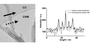
Image intensity measured along line sections perpendicular to TMV on CNM (dashed arrow) and CC (solid arrow) supports.
Image: Elsevier: UltramicroscopyD. Rhinow, M. Büenfeld, N.-E. Weber, A. Beyer, A. Gölzhäuser, W. Kühlbrandt, N. Hampp, A. Turchanin
Energy-filtered transmission electron microscopy of biological samples on highly transparent carbon nanomembranes
ULTRAMICROSCOPY , 2011, 111, 342-349
DOI: 10.1016/j.ultramic.2011.01.028External link
Cover Image of Small volume 7, Issue 7
Image: Wiley-VCH: Small
C. T. Nottbohm, A. Turchanin, A. Beyer, R. Stosch, A. Gölzhäuser
Mechanically stacked 1 nm thick carbon nanosheets: Ultrathin layered materials with tunable optical, chemical and electrical properties
SMALL, 2011, 7, 874-883
DOI: 10.1002/smll.201001993External link